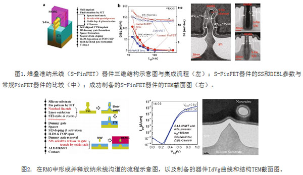
Recently, the Institute of Microelectronics of the Chinese Academy of Sciences’ Institute of Integrated Circuits Pioneering Process R&D (10th Room) has made new progress in the research of “Post-FinFET†devices with integrated circuits for 7nm and below. FinFET devices are the key architecture of the current 16/14-nanometer integrated circuit process technology. Because of the problem of channel electrostatic potential control, R&D of 7nm and below technology generations is facing serious technical challenges. Loop-gate nanowire devices have been recognized as the most promising ideal device structures for replacing FinFETs and applying at nodes below 7 nm due to their excellent electrostatic integrity and ballistic transport properties. However, due to its unique three-dimensional suspended nanowire channel and fully enclosed ring-and-gate structure, the gate-all-around nanowire device makes it difficult to directly use the existing quasi-plane technology to realize large-scale industrial integration. Therefore, the development of nanowire device integration technology compatible with the current 16/14nm FinFET mainstream process has become one of the important directions for the research of integrated circuit precursor technology in the “Post-FinFET†era. Under the support of the National Science and Technology Major Project 02 “16/14 nm Basic Technologyâ€, the microelectronics has achieved a number of important achievements in the research and development of the mainstream 16/14 nm all-gate high-k metal gate FinFET process technology. Ten-chamber researcher Yin Huaxiang's team has innovatively proposed two nanowire device integration technologies: stacked quasi-nanowire device (S-FinFET) technology and post-nanowire channel release technology in replacement gate (RMG), which has attracted wide attention in the industry. . Stacked quasi-nanowire devices (Figure 1) combine the industrial manufacturability of conventional FinFET devices with the channel electrostatic potential control similar to conventional nanowire devices. The researchers successfully fabricated a device with a minimum physical gate length of 14 nm on the microelectronics lead process R&D platform. The SS and DIBL parameters were 75mV/dec and 62mV/V, respectively, and the parameter distribution was close to the conventional FinFET device. The results were published in the 2015 Nanoscale Research Letter and have been highly recommended by reviewers, saying "it may be one of the important technologies for the next generation of FinFET technology." The nanowire channel post-release technology in the replacement gate (RMG) (Figure 2) has broken through the process constraints that have plagued the industry, academia, and research communities for achieving large-scale industrial integration of nanowire devices, and has been maximally compatible with existing FinFET baseline processes, achieving high-k The uniform integration of metal gates can be applied to high-density circuit integration and has important practical value. The technology was successfully fabricated on a pilot development platform for microelectronics. The integrated device has a nearly ideal elliptical topography channel and excellent subthreshold characteristics. The results were reported on IEICE Electronics Express in 2015. Solar Flood Light,Solar Led Flood Lights,Solar Powered Flood Lights,Solar Powered Security Lights Guangdong Smart Street Lighting Co., Ltd , https://www.gdfldlight.com