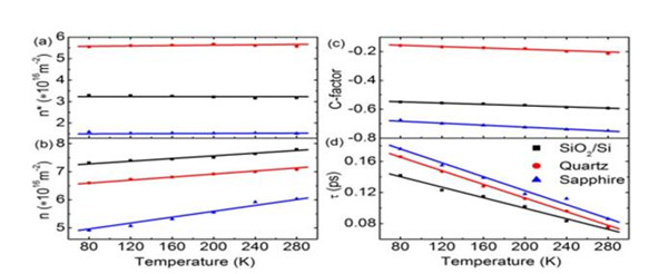
Recently, the research team of Xu Wen, a researcher of the Institute of Solid State Physics, Chinese Academy of Sciences, and the researchers of the Chinese Academy of Engineering Physics cooperated to apply terahertz time-domain spectroscopy (0.2-1.2 THz) and Fourier transform spectroscopy (2.5-6.5 THz) studied the terahertz photoelectric characteristics of single-layer MoS2 on different substrates. Related achievements were published in Optics Letters with the title of Substrate-induced electronic localization in monolayer MoS2measured via terahertz spectroscopy. In recent years, single-layer MoS2 has become a popular material in the fields of electronics and optoelectronics research, and its unique valley electronics characteristics make it potentially useful in the field of information technology. From a physics point of view, the most interesting feature of single-layer MoS2 is that the electron energy is approximately degenerate near the K and K 'points in the energy band, but the pseudospin directions of the electrons are opposite in the vicinity of these two points. Therefore, single-layer MoS2 can be used to study novel physical phenomena such as valley Hall effect, valley magnetic moment and valley light polarization. Similar to traditional thin-layer semiconductor devices, single-layer MoS2-based electronic and optoelectronic devices are usually placed on a substrate. The substrate introduces additional impurities, phonons, and interface scattering, which leads to the localization of the electrons in the single-layer MoS2, affecting the electrical and optical performance of the device. Therefore, studying the basic physical properties of single-layer MoS2 on different substrates is of great significance for the preparation and application of related devices. This is the main purpose and motivation of this research. Researchers have studied the terahertz optical properties of a single layer of MoS2 on three commonly used substrates (such as sapphire, quartz, SiO2 / Si). Since the terahertz photon energy (1 THz = 4.13 meV) is much smaller than the forbidden band width of the single-layer MoS2 (about 1.75 eV), THz irradiation will not excite photogenerated carriers and induce exciton effects in the sample, so THz can be used Spectroscopic techniques to study the free carrier characteristics of single layer MoS2. In addition, the localized information of the electrons in the sample can be obtained by studying the relationship between the real and imaginary parts of the photoconductivity of the sample with frequency. This is a physical characteristic that is difficult to measure directly in conventional electrical transport experiments. The study found that the relationship between the real and imaginary parts of the sample photoconductivity with frequency does not match the conventional photoconductivity (Drude formula), but it can well meet the Drude-Smith formula considering electron backscattering or localization effects. . Through the fitting of experimental data and theoretical formulas, optical measurements obtained the key material physical parameters such as the electron concentration, electron relaxation time (or mobility), electron localization factor of the sample, and their temperature-dependent (80-280 K) Change relationship. Related research is based on terahertz spectroscopy, which provides new ideas and ways to understand the influence of substrate materials on the physical properties of two-dimensional materials. The research was supported by the Ministry of Science and Technology, the National Natural Science Foundation of China, etc. Figure 1. Monolayer MoS2 on three different substrates: (a) effective electron concentration, (b) electron concentration, (c) electron localization factor, and (d) electron relaxation time as a function of temperature. The experimental results were measured by terahertz time-domain spectroscopy. Figure 2. The relationship between the real part of the photoelectric conductivity of a single layer of MoS2 on SiO2 / Si, sapphire, and quartz substrates at room temperature as a function of frequency. The low-frequency results are measured by terahertz time-domain spectroscopy, and the high-frequency results are measured by terahertz Fourier spectroscopy.
Resistance strain gauge is a kind of sensitive element by using resistance-strain effect to transform the strain of specimen into resistance change. It is the most widely used strain test element. The load cells used in weighing and measuring field mainly include resistance strain gauge type load cells, capacitance type load cells, vibrating string type load cells and so on, most of them are resistance strain gauge type load cells.
The resistance strain gauges produced by our company has the advantages of long liability and good uniformity, the functions of creep and temperature self compensation, suitable for batch production of alloy steel, aluminum ally and stainless steel load cells with high accuracy, and for producing other load cells and force and strain measuring elements.
High Temperature Strain Gauges,Strain Gauge,Foil Type Strain Gauge,Precision Strain Gages SHANDONG JINZHONG SCIENCE & TECHNOLOGY GROUP COMPANY LIMITED , https://www.chinagoldbell.com
