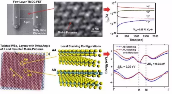
With the continuous application of new two-dimensional semiconductor materials such as graphene, molybdenum disulfide (MoS2), and tungsten selenide (WSe2) in the field of nanoelectronic devices, the charge trapping process inside two-dimensional materials has gradually received more attention. . On the one hand, people worry about whether this charge trapping process will affect the reliability of the device itself. On the other hand, they are constantly exploring whether they can use the internal characteristics of two-dimensional materials to create a new multi-bit memory device. Or analog adjustable memory. For this problem, the team of Professor Liang Xiaogan of the University of Michigan recently studied the phenomenon of abnormal charge trapping and memory characteristics of multilayer tungsten selenide (WSe2) transistors. This work shows that in a transistor made of multiple layers of tungsten-selenide that is mechanically exfoliated, they can excite multiple charge-trapping states with large spacing, long hold times, and analog tunability. However, they did not observe similar electrical phenomena in molybdenum disulfide (MoS2) with a similar material structure. The unique charge trapping characteristic of the tungsten selenide transistor is mainly attributed to the interlaminar deformation induced by mechanical exfoliation on the multilayered tungsten disulphide cutting surface, and these deformations can further spontaneously form bipolar charge trapping sites. They further supported this conclusion through various methods such as surface characterization, charge retention characteristics measurement at different temperatures, and density functional theory calculations. In addition, the study also shows that charge trapping states excited in different tungsten selenide transistors can be uniformly calibrated and stored as multi-bit data in memory devices. Through this research, they have gained a deeper understanding of the charge storage mechanism in two-dimensional semiconductor materials and further demonstrated that the observed charge trapping states can be used to implement new low-cost analog memory device technologies. This result was recently published on the ACS Nano. The first author of the article was Mikai Chen, a doctoral student at the University of Michigan.
Shear Beam Load Cells are widely used where operators need to measure compressive forces. The core component of a shear beam load cell is a spring element. This element is a piece of metal that is elastically deformed under load and recovers the moment the load is removed.
The (single-ended) shear beam is designed for low profile scale and process applications. The shear beam capacities are from 100kg to 50t. One end of the shear beam contains the mounting holes while the opposite end is where the cell is loaded. The load cell should be mounted on a flat smooth surface with high-strength hardened bolts. The larger shear beam cells have more than two mounting holes to accommodate extra bolts to keep the hardware from stretching under stress load.
Load Cell Central,Shear Beam Load Cells,Larger Shear Beam Cells,Load Cell Measure Compressive Forces Zhejiang Nanhua Electronic Technology Co., Ltd , https://www.nhloadcells.com